Fourbit, 4-bit homebrew CPU
Since
I was born in mid eighties, I've never experienced real 74xx build. Few
gates here and there was common, but lager designs were practicaly
uneeded - as microcontrollers, CPLDs or FPGAs replaced need for such as
work.
But my posession in vintage systems and desire to understand
inner working principles of modern devices brought me to design of
simple CPU made of simple 74xx devices.
CPU design
CPU
is not that complicated circuit, if we keep goals simple - so no
hardware multipliers, few registers, no fancy addressing modes. Such as
CPU is not particular useful, as even old 8080 outperforms this easily,
but performace is not primary goal now.
Basically, CPU does simple
things - moving data from/to memory locations and making operations on
it. Program flow should be allowed to change and IO latches are needed
for real world operation.
Registers
Registers
are elemntary part of CPU design. Thay serve as most used and useful
memory locations, source or target of most of instructions. We will
have a few registers in our design.
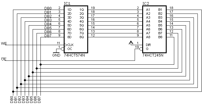
Heart
of register is latch 74HCT574. It latches data from data bus DB on
rising clock of WE signal. Passing this data to DB is controlled by OE
signal, using bus driver 74HCT245. Theoretically we can use OC signal
of 574, but data should be accessible even when output is not brought
to DB. That is why two ICs are needed to build single register.
We can have a lot of registers on single bus, with WE and OE signals
for each one register.
ALU
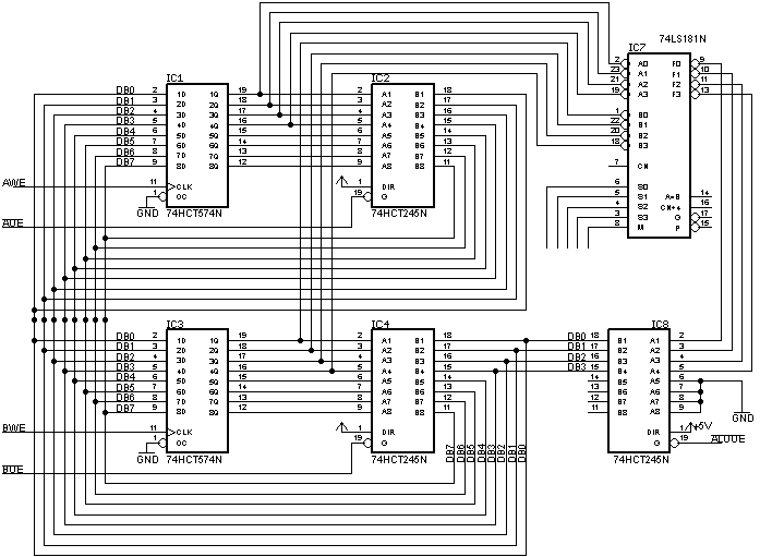
Adding
ALU is quite simple task, thanks to 74181 developed in late 60's/start
of 70's. It is 4-bit wide ALU, capable of performing almost all common
logical and arithmetic operations.
Let's put two registers together, add 74181 and serve with single bus
driver.
Nothing
special here, but this starts to be quite useful. We have two registers
(A and B), controlled by respective OE and WE signals, ALU, with
operation controlled by signals on M and S1 to S4 signals (for more
details see 74181 datasheet). Because 74181 doesn't have tristate
outputs for connecting to DB, bus driver is needed here. So, data in
both registers (accessible from DB) can be passed through ALU and put
on DB again.
Imagine we want to do this sequence: put data to A,
another data to B, perform ALU operation and put into A again. We need
to put A data on bus, assert and release AWE, then put B data on bus,
assert and release BWE. In the meantime, ALU does its job (it is only
combinational logic) and on F1 to F4 outputs is result. We can assert
ALUOE to put result on bus. To write it to A register, asserting AWE is
needed... but wait. If we asert WE, latched data (ALU result) appears
on data lines of A register, ALU changes its output and this is (or may
be) transferred to A register.
That's why third register is needed.
Lets call it T - temporary register. After putting ALU content on bus,
we write it to T register and then (when ALU output is securely saved)
to A register again.
PC
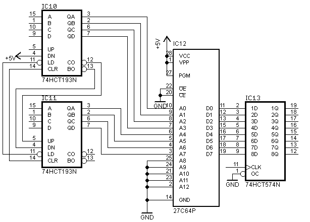
Let's
focus now on another important part of CPU, program counter - PC. It's
main job is to increment whenever new instruction is needed or set to
value when program jump is to be made.
Nothing
special again. Two chained 74HCT193 counters, EEPROM memory holding
program and instruction register (IR). It holds current instruction
byte until it is fully executed.
Preset inputs of counters (A, B, C
and D) are connected to BD, in order to allow direct change of PC
(program jump). Otherwise PC changes after each single instruction by
CLOCK UP signal (pin 5).
Instruction decoder, part one
PC
and registers with ALU are muscles of CPU, doing hard work, but it
needs a brain - to decide when and how to change control signals.
Instruction decoder does this job. Now starts the real fun and messing
with 74xx logic.
Before actually building instruction decoder, it is neccesary to decide
which instructions we are going to decode.
Instructions
For this computer, I decided to use only three instructions:
1, load direct data to A
2,
move data from source to destination. Source can be A, B, RAM or input
registers; destination can be A, B, PC, RAM or output registers.
3, do ALU operation between A and B, move result to A
Allowing
PC to be result of move allows jumps. You can transfer input data from
IO port to RAM in single instruction. From hardware point of view, RAM
is treated as another register, with address bus connected to B
register. So, B is address pointer for RAM operation. Some move
instructions have to affect on registers or memory. Example is move A
to A. This could be equivalent of NOP instruction.
There is no dedicated indirect addressing register, no stack, no
interrupts.
MSB
of instruction determines whether instruction is LDI. We need to waste
only one bit for this, so 7 bits are used as immediate data. As
immediate data are one of sources for jump instructions, this allows
addressing 128B of program ROM. In fact, data from ALU (computed jump)
can be used for jumping, but this address is only 4 bits wide, allowing
addressing 16B of ROM, leaving this option as not very useful.
If
MSB is zero, next bit determines MOV or ALU instruction - notice how
this step by step description determines real operation of instruction
decoder.
Instruction timing
Instructions are divided into single steps. In our case, we will have
for steps, let's call it machine cycles.
M1: load instruction to IR and put source data on DB
M2: load source data from bus to T register
M3: put data from T register on DB
M4: load data from DB to destination, increment PC
Black rectangles denote active (high) level. CLK is incoming clock
signal. Whole instruction is done in eight cycles.
Instruction set is simple:
|
7 |
6 |
5 |
4 |
3 |
2 |
1 |
0 |
| MOVI |
1 |
IMMEDIATE DATA |
| MOV |
0 |
0 |
SRC |
DST |
| ALU |
0 |
1 |
X |
M |
S3 |
S2 |
S1 |
S0 |
If actual instruction is MOVI, source data is lower 7 bits from IR,
destination is A
If actual instruction is MOV, source data is determined by IR[3..5] and
destination by IR[0..2]
If actual instruction is ALU, source data is from ALU bus driver,
destination is A
This gives us first clue about instruction register operation.
Notice
leading edge of M2 comes while M1 is still high. This overlap is needed
to securily write data into T register. The same goes for M3 and M4.
Building
clock circuit is quite simple. We need D-flip-flop, dividing input
signal by two, giving with incoming clock four possible states. Those
states are decoded by simple AND logic. To achieve 1:1 duty cycle of
incoming clock signal from 555 timer, second D-FF is used.
Instruction decoder, part two
Knowing
what a how to decode, we can proceed in design of instruction decoder.
Let's start with most complicated instruction, MOV. We need to select
source register during phase M1 and put on bus - so OE signal of
selected register should be active during M1 phase. We can use 74HCT138
1-of-8 decoder. Fortunately it has three chip select pins, two of them
inverted. We can connect those two to IR[7] and IR[6] signals, thus
activating during MOV instruction. Third, high active, select pin is
connected to M1 signal. The same goes for selecting destination
register, with the exception that third chip select pin goes to M4
signal. To complete MOV instruction, we need to take care of T
register. OE of T register will be active during M3 and WE during M2.
MOVI and ALU instructions are very alike, except of that first one
select IROE signal, while former selects ALUOE signal during M1. AWE
(write to A register) is active during M4 for both instructions.
Fourbit
schematics in PDF
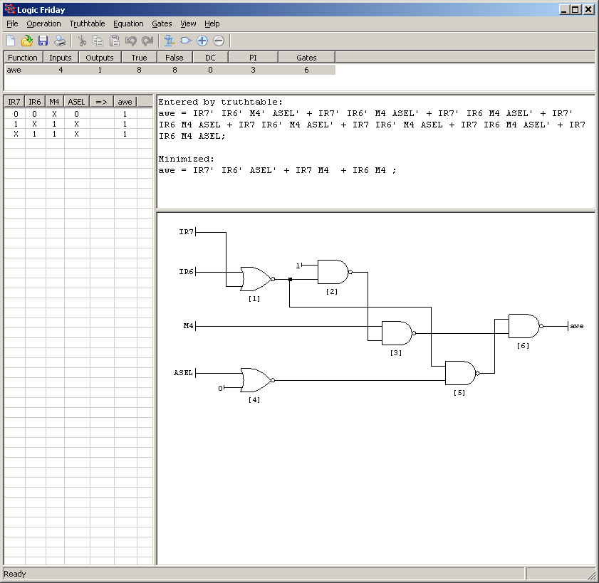
IC20,
IC21 and IC22 does this job - generates IROE and ALUOE signals, as well
as AWE signal. For this purpose I used simple looking, but useful
software, Logic Friday.
I generated this truth table for AWE signal
and software minimized this table into equations and generated circuit
of logic gates doing the same job.
I did the same for IROE and ALUOE signals. Voila, instruction decoder
is done.
We
need to make jumps conditional in some way. I decied to use register B
for this purpose. When it's content is 0xF, jump (MOV to PC) is
executed as NOP.
Notice, on final schematics, signal M3 is not
used at all. It is needed for latching output of T register, but M1 is
used, as driver expects negative logic and M3 is only inverted M1.
Input/output ports
The
only thing not described for now is IO part. We have two signals from
138 decoders, so all is needed is double 4-bit bus driver (IC25) for
input ports and two 4-bit wide latches as output ports (IC26, IC27).
Programming
As
our CPU is basically done, we need to program it to make something
useful. Lets start with simple program - emulation of four NAND gates.
MOV IA,A
; move data from input A to register A
MOV IB,B
; move data from input B to register B
ALU NAND
; do NAND operation
MOV A,PA
; move data from A (ALU result) to port A
MOVI 0
; move zero to A
MOV A,B
; move this zero to B
MOV A, PC
; jump to zero
Quick hand assembly gives this output
0x20
0x29
0x54
0x04
0x80
0x01
0x02
That is ready to be burned into EEPROM. I used Genius G540 programmer -
really low cost, but it does its job.

Result, or 7400^2 to 7400^x
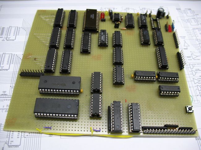
Circuit
was built on perfboard with dimension cca 18x18cm. Current consumption
is about 180mA, majority of this is drawn by 74181 and 74175 in plain
old TTL technology.
Clock
speed is determined by C1 capacitor. For 1uF, clock generator ticks at
about 80Hz, giving 10Hz execution speed. For no capacitor, oscillator
works at frequency given by stray capacitance, resulting in cca 57kHz
execution speed. Yes, whopping 57,000 instructions per second.
Processor,
or single board computer, works as expected. I wrote emulation program
that allows emulation of four NAND gates, basically acting like single
7400 IC - let's call it second generation 7400. This may seem to be
trivial and unusable (OK, it IS ususable), but limited number of those
(second generation) 7400 ICs allows to build another CPU that allows
emulation of another 7400 - third generation 7400. We can continue
indefinitely, building more and more generations of 7400 ICs. If we
look at last generation of 7400, we can zoom at its basic parts - there
would be 7400 computers, built from 7400 computers - something like
zooming on fractals. Fractal 7400 computer, that's it.
This project was finished as entry for 7400 design contest.
Schematics of my board in PDF format is here
(Resistors are 12kOhm, C2 is 100nF, C1 depends on needed clock)
More images to see in my Picassa
album
Or short video of NAND emulation here
Updated 29.10.2012
Back to home